

| Specification of the sample design |
| Technology |
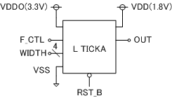
| Core voltage | 1.8V |
| IO voltage | 3.3V |
| Fabrication technology | CMOS 180nm, 5-Metal, available for mixed signal circuits |
| Architecture |
| Module Name | Function | Implementation Method |
|---|---|---|
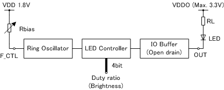
| Rbias | Variable resistance to control the clock frequency | External component |
| Ring Oscillator | Current Control Oscillator | Full-custom circuit |
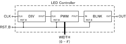
| LED Controller | Pulse width modulation and flicker circuit | Standard cell |
| IO Buffer | LED driver° Open drain, Max.12mA°ň | IP provided by the manufacturer |
| LED | Controlled LED | External component |
| RL | Adjusting load resistance | External component |
| IO port |
| Port Label | Attribute | Function |
|---|---|---|
| F_CTL | Analog Input | Frequency control |
| WIDTH[3:0] | Digital Input | Brightness control |
| RST_B | Digital Input | Reset |
| OUT | Digital Output | LED drive |
| VDDO | Power | 3.3V Power |
| VDD | Power | 1.8V Power |
| VSS | Power | Ground |
Copyright (C) 2016- Akio Kitagawa, Kanazawa Univ.