Place and route (P&R) tools uses a physical technology information written in the technology file (If you find the file "rohm018_icc.tf" in your working directory, you may skkip this setting). Make a symbolic link from the technology file for P&R tool (Synopsys IC compiler) to your working directory.
vlsi> cd  ~/d
vlsi> ln  -s  kyoto/templete/rohm018_astro_kyoto-u.tf  rohm018_icc.tf
Execute the following command line to start IC compiler.
vlsi> setlic
      Choose the number of Synopsys IC compiler.
vlsi> cd  ~/d/ICC
vlsi> icc_shell  -gui  -64bit (Don't use &)
- Menu: File > Create Library... and create library with the next configuration.
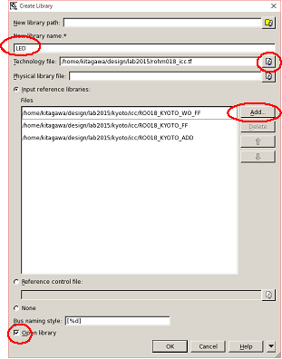
- Technology file = rohm018_icc.tf
- Click "Add... button" and choose the library files in "../kyoto/icc" directory. The following files are required.
- RO018_KYOTO_WO_FF //Combinational logic library
- RO018_KYOTO_FF //Flip-Flop library
- RO018_KYOTO_ADD //Power line, Filler patterns
- Check the checkbox of "Open library"
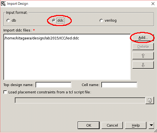
- Menu: File > Import Designs...
- Input format = ddc
- Click "Add..." and choose "led.ddc"
- Click the OK button.
- If the netlist of the target circuit is successfully read in the IC compiler, the layout window is opened.
- Menu of layout window: Preroute > Derive PG Connection...
- Input the name of the power net and pins
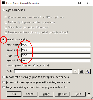
- Execute the next command line for the command prompt of "icc_shell> ". The net which have a fixed logic value is tied to the net of VDD or VSS by this command.
icc_shell> derive_pg_connection -tie -power_net VDD -ground_net VSS
- Menu of layout window: Floorplan > Write Pin/Pad Physical Constraints...
- Output file name = led_pin_core.tcl
- Click the OK button.
- "led_pin_core.tcl" is created. This file is used to give a constraint conditions of IO-pin alignment.
- You can edit this file to specify the IO-pin location to your design.
Contents of led_pin.tcl
set_pin_physical_constraints -pin_name {WIDTH[3]} -layers {METAL3} -width 0.28 -depth 0.28 -side 1 -order 1
set_pin_physical_constraints -pin_name {WIDTH[2]} -layers {METAL3} -width 0.28 -depth 0.28 -side 1 -order 2
set_pin_physical_constraints -pin_name {WIDTH[1]} -layers {METAL3} -width 0.28 -depth 0.28 -side 1 -order 3
set_pin_physical_constraints -pin_name {WIDTH[0]} -layers {METAL3} -width 0.28 -depth 0.28 -side 1 -order 4
set pin_physical_constraints -pin_name {CLK}      -layers {METAL3} -width 0.28 -depth 0.28 -side 1 -order 5
set_pin_physical_constraints -pin_name {RST_B}    -layers {METAL3} -width 0.28 -depth 0.28 -side 1 -order 6
set_pin_physical_constraints -pin_name {OUT}      -layers {METAL4} -width 0.28 -depth 0.28 -side 2 -order 1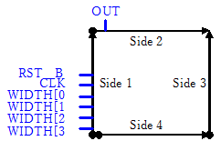
In this figure, the square is a circuit boundary and the direction of an arrow shows an order of the pins. Instead of "-order", you can use "-offset" to specify the distance from the starting point on each side. The width of the pin and length of the pin are specified by using "-width" and "-depth". You can increase the width and depth of IO pins, because "0.28" micrometer is a minimum size in the design rule.
- After editing "led_pin.tcl", the Menu of layout window: Floorplan > Read Pin/Pad Physical Constraints...
- Menu of layout window: Floorplan > Create Floorplan...
- You can specify the shape of the circuit boundary and the layout method of the cell.
- NOTE: Large "space between core area and terminals" is suggested, because this area is used as a power-rings area around the core circuit.
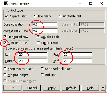
- Click the OK button or Apply button.
- The boundary in which the standard cell will be placed and the outer shape of the standard cells are shown in the layout window. Check the location of the IO pins which are shown as cyan square.
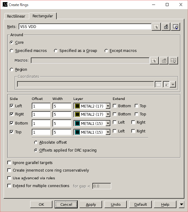
- Menu of layout window: Preroute > Create Rings...
- Choose "Rectangular" tab and set as following figure.
- The power rings supply the power to all standard cells.
- Click the Apply button.
- If you want to adjust the line width or position od the VDD and VSS rings, you can erase the rings by clicking the "Undo" button and retry.
- Click the "Cancel" button to finish the "Create Rings" form.
- You can delete the power wires and via connections by using a right-click menu, and retry the creation of the power rings.
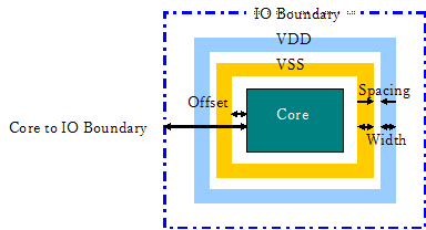
- You may create a strap on the power ring, when the core area is large. The strap helps to decrease the resistance of the power line to the cells placed in the midmost of the core.
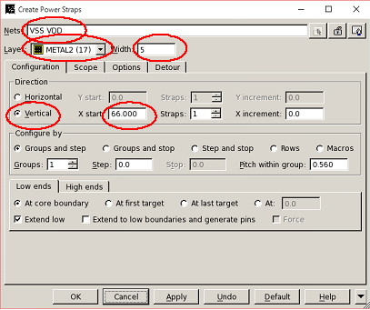
- Preroute > Create Power Straps...
- For example, Number of strap = 1, Direction = Vertical.
- Click the Apply button.
- You can retry the creation of the straps. Delete with the "Undo" button and change the value of ��X start, X increment, Y start, and Y increment.
- Click the "Cancel" button to finish the "Create Power Straps" form.
- Preroute > Create Power Straps...
- Execute the following command line for the prompt of "icc_shell> "
- The METAL1 and METAL2 layer is used for the power connection and the placement of the cells under the power strap is prohibited.
icc_shell> set_pnet_options -complete {METAL1 METAL2} - File > Save Design...
- Menu of layout window: Placement > Core Placement and Optimization...
- Execute the following command line for the prompt "icc_shell> "
- The tie cells are inserted to make the wire whose logic value is fixed.
icc_shell> connect_tie_cells -objects [get_cells * ] -obj_type cell_inst -tie_high_lib_cell ROHM18TIEHI -tie_low_lib_cell ROHM18TIELO
- Menu of layout window: Preroute > Derive PG Connection...
- IC Compiler replaces the cells to optimize the driving power of the cell. Therefore, the power connection is sometimes cancelled and must be reconfigured after the placement.
- Menu of layout window: Preroute > Preroute Standard Cells...
- Click the OK button to complete the power connection.
- Execute the following command line to fix the notch of the wire.
icc_shell> set_route_options -same_net_notch check_and_fix
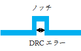
- Execute the following command line to create the clock tree before routing other nets.
icc_shell> clock_opt -fix_hold_all_clocks -no_clock_route
NOTE: The clock tree network is required to deliver the consistent timing of the clock signal. Therefore, routing of the clock tree is carried out previous to other networks. - Menu of layout window: Finishing > Insert Standard Cell Filler...
- The filler cell is a blank cell, but it works just a path of the power line and well and body ties.
- The seven filler cells are provided, Set these cell names into "Master cell name" and put a check the checkbox of "METAL1" in "Avoid fillers under layers" frame in the Insert Standard Cell Filler" form.
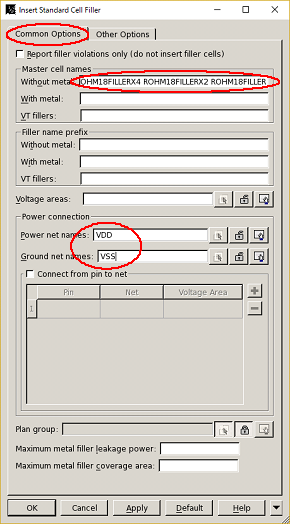
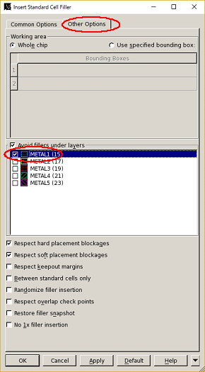
Master cell names (Use space as a delimiter)
ROHM18FILLERX64
ROHM18FILLERX32
ROHM18FILLERX16
ROHM18FILLERX8
ROHM18FILLERX4
ROHM18FILLERX2
ROHM18FILLER
- Execute the following command line for the prompt "icc_shell> " to prescribe an antenna-rule to IC compiler.
icc_shell> source  ../kyoto/icc/tcl/antennarule_tcl
icc_shell> set_route_zrt_global_options  -default  true
icc_shell> set_route_zrt_detail_options  -antenna  true  -antenna_on_iteration  2  -diode_libcell_names  {ROHM18DIODEX1 ROHM18DIODEX2 ROHM18DIODEX4}  -insert_diodes_during_routing true  -max_antenna_pin_count  -1  -port_antenna_mode  top_layer  -antenna_fixing_preference  use_diodes  -default_port_external_gate_size  0.45  -default_port_external_antenna_area  5
NOTE: The length of the metal connected to gate electrode of MOSFET is restricted by the antenna rule to prevent ESD (Electrostatic Discharge) damage in the fabrication process.
- Execute the following command line to make the clock tree.
icc_shell> route_zrt_group -all_clock_nets
- Menu of layout window: Route > Auto Route...
- Check the error messages in the IC Compiler window or the terminal in which IC compiler was invoked. If there is no error, you can find the following messages.
Total number of DRCs = 0
Total number of antenna violations = 0
Total number of voltage-area violations = no voltage-areas defined
- Execute the following command line to run the detailed router.
icc_shell> route_zrt_detail -incremental true
- Menu of layout window: Route > Optimize Wire Via...
- If the error occurs, retry the detailed routing and the optimization several cycles. If the error is still remaining, go back to the floor plan and decrease the value of "Core utilization". The spaced pin alignment sometimes leads to a positive result.
- Execute the following command line to check the violation of the antenna rule.
icc_shell> verify_zrt_route -drc false -antenna true
- Menu of layout window: Preroute > Derive PG Connection...
- The power net is reconfigured after the optimization of P&R.
- Menu of layout window: Preroute > Preroute Standard Cells...
- The connections of the power and ground of the standard cells are wired up again.
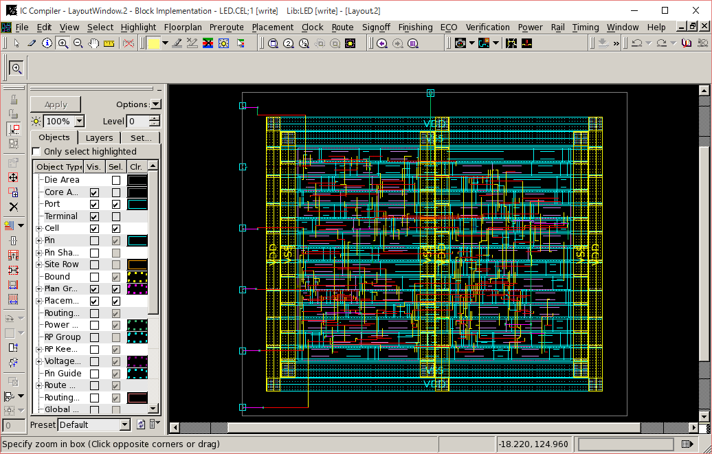
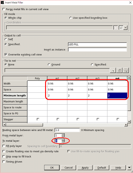
- Menu of layout window: Finishing > Insert Metal Filler...
- This command inserts the dummy metals in the METAL1 - METAL4 layers to prevent the violation of the density rule. The fab maker imposes the density rule to increase the precision of the planarization process.
- Menu: File > Save Design...
- Click the "Save All" button.
- Execute the following command line for "icc_shell> " prompt to assign the layer number defined by the fabrication company.
icc_shell> set_write_stream_options -map_layer ../kyoto/template/A2GDS.map -child_depth 99 -output_pin {text geometry} -output_design_intent - Execute the following command line to format LVS netlist.
icc_shell> define_name_rules  verilog  -allowed "A-Z0-9_"  -type net
icc_shell> change_names  -rules  verilog  -hierarchy
- Menu: File > Export > Write Verilog...
- Uncheck the checkbox of "Output physical only cells" to stop listing of the physical cell which is not significant in the schematic.
- Give a different file name from the netlist created by the logic synthesis. (ex. led=pr.v)
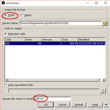
- Menu: File > Export > Write Stream...
- Add ".str" and ".gds" for the file extension. (ex. LED.str)
- A GDS-II file is exported. This file format is accepted by the semiconductor manufacturer and supported by most layout tools.
- Menu: File > Exit

