In this section, we will use Cadence Virtuoso (IDE) + Mentor Calibre (DRC).
vlsi> setlic
      Choose the number of Cadence IC.
vlsi> setlic
      Choose the number of Mentor Calibre.
vlsi> cd  ~/d
vlsi> virtuoso &
CIW(Command Interpreter Window) is started.
- Menu of CIW: Tools > Library Manager...
- Menu of Library Manager: File > New > Library...
- Library name = Lticka (or any name), Directory to save = libraries (or any directory)
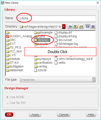
- Check the checkbox of "Compile an ASCII technology file" in Technology File for New Library form
- Click Browse... button in Load Technology File form.
- Choose "rohm180technology_ic6.tf". This file is a Technology file formatted for Cadence Virtuoso.
- The library "Lticka" is added to Library Manager.
- Menu of Library Manager: File > New > Cell View...
- Cell name = rosc, Type = schematic, Open with = Schematic XL
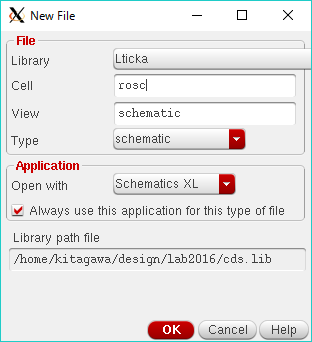
- Draw the schematic of the ring VCO (Example of the schematic entry)).
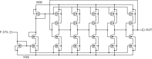
NOTE: A ring oscillator is composed of the odd numbered stages of the inverters with the feedback loop. The oscillating frequency of the ring oscillator depends on the number of stages and the sum of the delay times of the inverters. The delay time of the inverters can be controlled by the current controlling transistors which are connected to the inverter in series. This circuit is often used as a voltage controlled oscillator (VCO). The current of the current controlling transistors controlled by the current of the current mirror circuit. In conclusion, the frequency of the ring VCO is controlled by controlling the current flowing into F_CTRL.
Components (Shortcut = i)
Library Cell View Description vdecRO180PDK nmos18 hspiceD 1.8V n-ch MOSFET model vdecRO180PDK pmos18 hspiceD 1.8V p-ch MOSFET model analogLib vdd symbol analogLib vss symbol NOTE: The symbol of the input pin and output pin are brought up by the shortcut key "p".
Properties of MOSFETs (Shortcut = q)
Type L W Multiplier (Number of parallel connections) n-ch MOSFET 180n 1u 1 p-ch MOSFET 180n 2u 2 Estimate the AD (Drain area), AS (Source area), PD (Drain periphery), PS (Source periphery) by the following formulae and input them to the property form of MOSFETs.
AD = AS = 0.5um*W (ex. If W=1um, then AD = AS = 0.5p)
PD = PS = 1u + W (ex. If W=1um, then PD = PS = 2u)
- Menu of schematic editor: Create > Cellview > From Cellview...
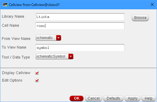
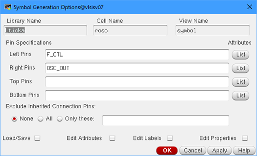
- Create a new cell named "tb_rosc" in the Library Manager
- Draw the schematic of the testbenchˇĘExample of the schematic entryˇËˇŁ
- Resistance value = rbias, The value of rbias will be assigned later by Test Editor.
- Label the output line.
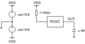
Components (Shotcut of Instance = i, Shortcut of Property = q)
Library Cell View Description Lticka rosc symbol analogLib res symbol Resistance = rbias analogLib cap symbol Capacitance = 6f analogLib vdc symbol DC Voltage = 0.9 analogLib vdd symbol analogLib vss symbol analogLib gnd symbol
- Menu of Library Manager: File > New > Cell View...
- Adexl view is a view for the configuration of simulation settings.
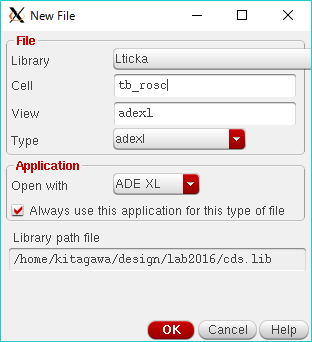
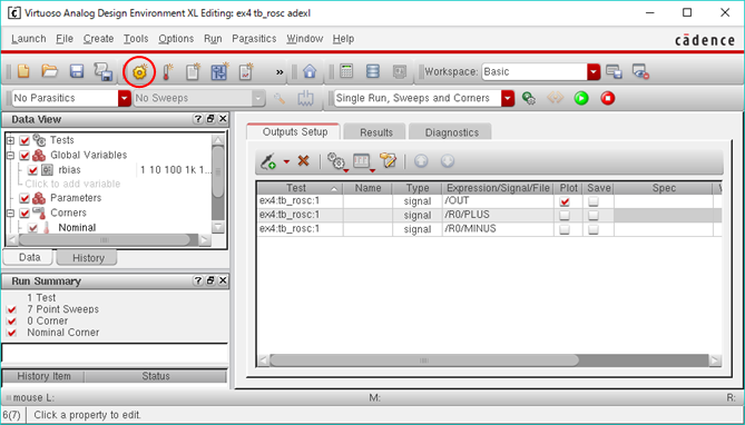
- Click Create Test (Icon of a gear) on the toolbar of ADEXL (Analog Design Environment XL). In the Choosing Design form, Library Name = Lticka, CellName = tb_rosc.
- Test Editor Window is started up.
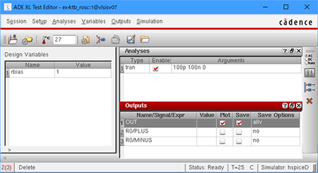
Settings in Test Editor
- Setup > Simulator...
- Simulator = hspiceD
- Setup > Model Libraries...
- Click <Click here to add model file> and '...' buton. Choose the model file name and the section as shown in the following table. NT and PT shows that the model parameters of n-ch MOSFET and p-ch MOSFET are typical (mean value), respectively.
Model File Section spice/hspice/bu40n1.mdl spice/hspice/bu40n1.skw NT spice/hspice/bu40n1.skw PT - Click <Click here to add model file> and '...' buton. Choose the model file name and the section as shown in the following table. NT and PT shows that the model parameters of n-ch MOSFET and p-ch MOSFET are typical (mean value), respectively.
- Setup > Environment...
- userCmdLineOption = -csfe
- Simulation > Convergence Aids > Initial Condition...
- Click the wiring "OUT" in the schematic, and set the initial voltage = 0.9 (see NOTE)
- Analyses > Choose...
- Analysis = tran, Start = 0n, Stop = 100n, Step=0.1n, Enabled
- Variables > Edit...
- Name = rbias, Value(Expr) = 1
- Outputs > Setup...
- Click From Design button.
- Click the wiring "OUT" in the schematic.
- Hit ESC to exit the setup mode.
- Click OK button on the Setting Outputs form.
- Simulation > Analog Options > Interface Options
- POST = ASCII(2)
NOTE: The oscillator is started by the perturbation, such as a noise, a change of temperature, and a transient in power-on. Before the transient analysis, the circuit simulator automatically calculates the initial condition, which is obtained from DC analysis for the static bias state, however, the initial condition calculated by the DC analysis includes no perturbation and the circuit keeps a initial state. In the simulation of the oscillator, the initial condition which is deviated from the DC bias condition should be provided to the simulator. In this example, the initial voltage of 0.9V was applied to the OUT node. The transient response time depends on the value of given initial condition.
- Setup > Simulator...
- Menu of Test Editor: Simulation > Netlist > Create
- The netlist is created and shown in the new window.
- Menu of netlist window: File > Save As...
- Directory = sim, Faile name = rosc.sp
- Edit the netlist to add the HSPICE directives.
- Add "*" at the beginning of the ARTIST and PSF line in .OPTION directive, and add .ALTER directives and .PARAM directives before .END directive.
vlsi> emacs rosc.sp &
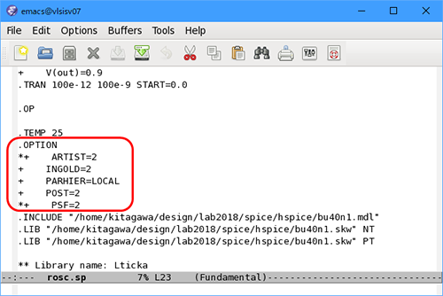
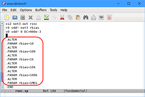
Note: The simulation is suspended at .ALTER directive and the parameter rbias is updated by .PARAM directive, thereafter the simulation is restarted successively.
- Execution of HSPICE simulation
vlsi>cd  ~/d/sim
vlsi> setlic
Choose the number of Synopsys HSPICE.
vlsi> hspice  rosc.sp

      .
      .
      .
      .
>info:         ***** hspice job concluded
The simulation has succeeded if you see "hspice job concluded". If an error occurs, check the file name and the revised netlist. - Chekeing the simulation result with CosmosScope.
vlsi> cscope &
- menu of CosmosScope: File > Open > Plotfiles...
- Shift-click to choose the files of the simulation results from rosc.tr0 to rosc.tr6, and click Openbutton.
- The signal-list window is appeared for each file.
- Choose the voltage signal v(out) and click each Plot button.
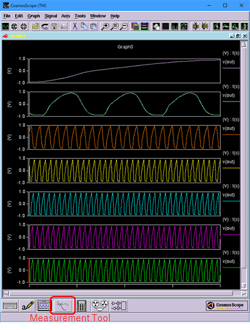
- The amplitude, phase and frequency of the simulation results is measured by using Measurenment Tool, which can be started with the toolbar button.

