The layout editor is included in the integrated development environment which you have already used for the schematic entry.
vlsi> setlic
      Choose the number of Cadence IC6.
vlsi> setlic
      Choose the number of Mentor Calibre.
vlsi> cd  ~/d
vlsi> virtuoso &
- Menu of CIW: Tools > Library Manager...
- Click "Lticka" in Library Manager
- Menu of Library Manager: File > New > Cell View...
- Cell = rosc, Type = layoutˇ˘Open with = Layout XL
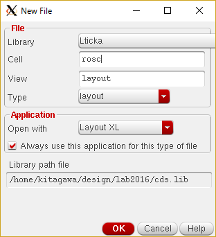
- The layout view of rsoc is added in Library Manager and Virtuoso layout editor is launched.
- Menu of Layout editor: Options > Display...
- The grid spacing is restricted by the design rules, which is determined in each layer. The grid spacing shown in the following table is based on the common factor of all layers. If you want to increase the density of the layout, please refer the detailed design rule.
Example of the grid and the snap setting
Grid Controls - Minor Spacing 0.02 Grid Controls - Major Spacing 0.2 Grid Controls - X Snap Spacing 0.02 Grid Controls - Y Snap Spacing 0.02 Snap Modes - Create anyAngle Snap Modes - Edit anyAngle 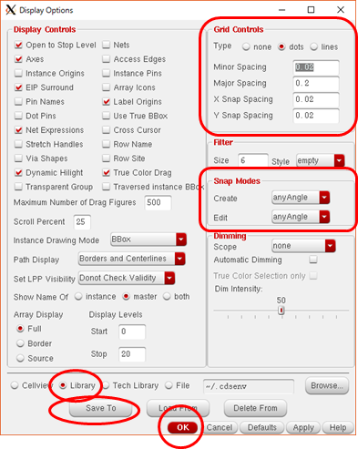
- Check the radio button on the form of the display options.
- Click "Save To" button and OK button.
- Display Stop Level (Numerical input-box) on the toolbar = 10
- The display stop level controls the display depth of the hierarchy. If you set larger value, you can see the detailed layout, but the display speed is decreased.
- Work Space = Basic

- The layout editor is accompanied by opening the schematic editor. Choose the transistors on the schematic editor to create the layout of the transistors.
- Do not choose too many transistors, because too many parts of the transistors are shown in the layout editor and you may fall into confusion. The 1-stage of the ring oscillator, which includes the four transistors, is adequate amount of the artwork.
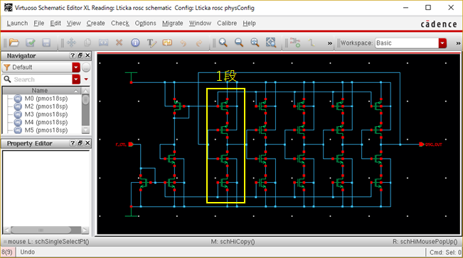
- Click "Generate Selected From Source" button of the toolbar on the bottom side of the layout editor.
- The layout patterns of the six transistors are shown in the layout editor, if you choose the four transistor's symbols on the schematic. The multiplier of the transistor's property means the number of the parallel connections of the transistors. You set the multiplier of p-ch MOSFET to two, therefore, the six transistors are generated for the four symbols.
Generate Selected From Source button

- Move the layout of the transistor close to the adjacent layout. The drain area or the source area of MOSFETs will be merged automatically and the abutting shape of two transistors will be created. (More detailed explanation)
Move button (Shortcut = m)

- If the transistors have both of a series connection and a parallel connection, create the abutting shape of the transistors through the following steps.
- Make abutting shape of the series-connected transistor first.
- Next, make abutting shape of two pairs of the series-connected transistors.
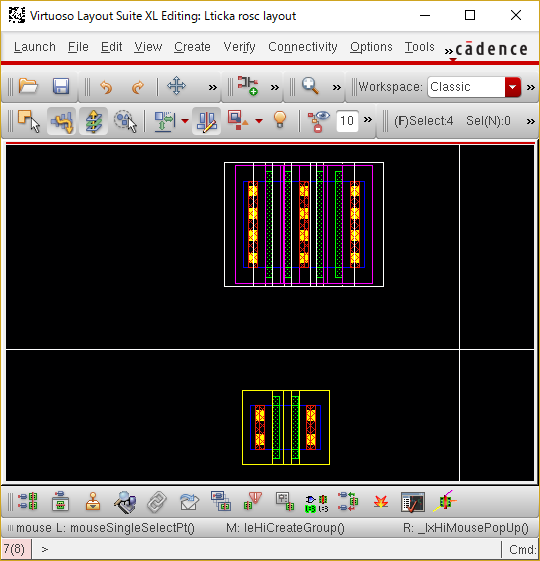
- Click "Create Group" button on the toolbar to group the n-ch MOSFETs
- Group the p-ch MOSFETs similarly.
"Create Group" button

- Basic operation to create a wire
- Click "Create Wire" button on the toolbar.
- Click the wire or the electrode of the MOSFET to tap.
- If you click the overlapping area of the multiple layers, choose the layer on "Choose Object to Tap" form.
- Move the mouse cursor to the destination point and double-click to finish wiring.
"Create Wire" button (Shortcut = CTRL + Shift + w)

- Make the gate connection.
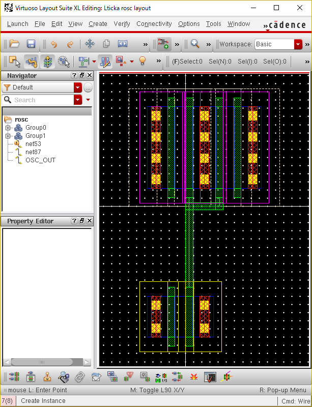
- Place the contact pattern to connect the gate poly-Si layer (GATE) and the first metal layer (METAL1).
- Press the i-key to call for the contact sandwiched between GATE and METAL1, and choose the CGATE in the layoutLib.
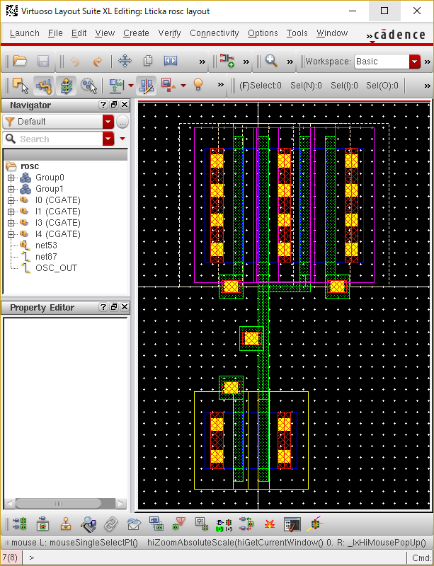
- Place the via-contact pattern to connect the first metal layer (METAL1) and the second metal layer (METAL2).
- Press the i-key to call for the via-contact (VIA1) sandwiched between METAL1 and METAL2, and choose the VIA1 in the layoutLib.
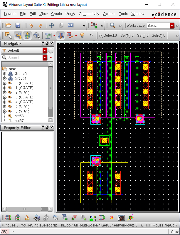
- Wire the electrodes of MOSFETs with METAL1 (red) and METAL2 (cyan).
- If you click the overlapping area of the layers, choose the layer on "Choose Object to Tap" form.
- If you want to change the width of the wire, after tapping the wire, right-click and choose "Options..." from pop-up menu. You can input the width of the wire in "Create Wire" form.

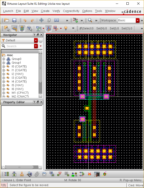
- Create the NWELL tie.
- Press i-key to call up the CNACT cell in layoutLib.
- In "Create Instance form", Rows = 2, Columns = 6, Delta Y = 0.48, Delta X = 0.48
- Place CNACT on the side of p-ch MOSFET.
- If the warning is issued about the values of Delta X and Y, ignore it.
- Create the P-Substrate tie.
- Press i-key to call up the CPACT cell in layoutLib.
- In "Create Instance" form, Rows = 2, Columns = 6, Delta Y = 0.48, Delta X = 0.48
- Place CPACT on the side of n-ch MOSFET.
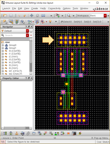
- Draw the NWELL around the NWELL tie (CNACT).
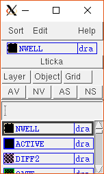
- Click the NWELL layer in LSW (Vertically long window).
- Menu of layout editor: Create > Shape > Rectangle (Shortcut = b)
- Clisk the diagonal point of the NWELL.
- Create the approximate size of the rectangle, then scaling it accurately by using the stretch button of the toolbar (Shortcut = s) and click the side of the rectangle.
- The gap between the NWELL of the well tie and the NWELL of the p-ch MOSFET will cause a design rule error.
- The short distance between the side of ACTIVE and the side of NWELL will cause a design rule error.
LSW
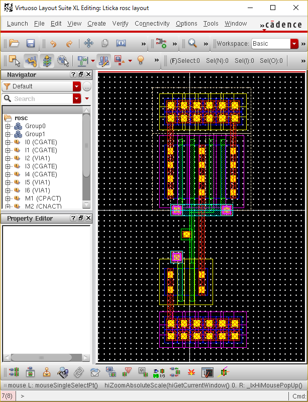
- Connecting the power line.
- Choose the METAL1 layer on LSW.
- Press b-key and click the diagonal point to create a rectangle of METAL1 over the CNACT pattern and the CPACT pattern.
- Click "Create Wire" button (Shortcut = CTRL + Shift + w) and connect from the source electrodes of MOSFETs to VDD(Power) or VSS(Ground).
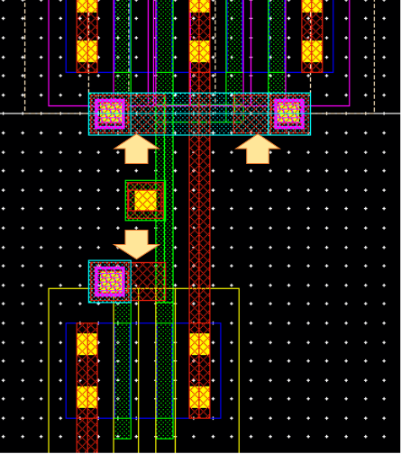
- Press b-key to create the rectangles of METAL1 and stack up it on the small metal area. If the area of the metal is too small, the design rule violation occurs.
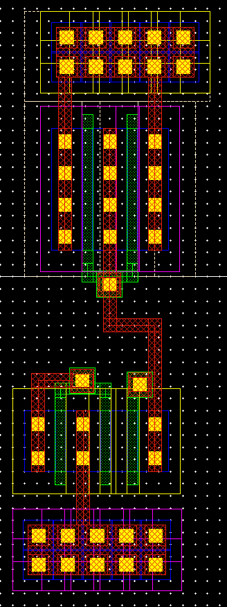
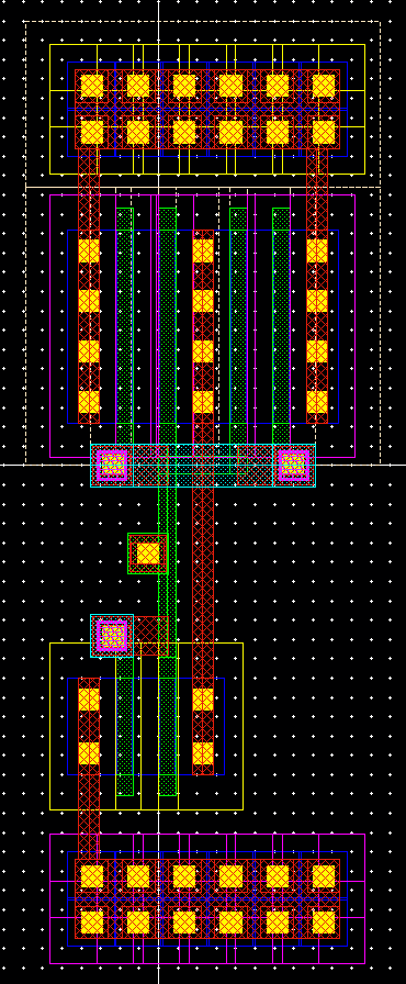
- Check your layout of the current-controlled inverter.
- Save your design.
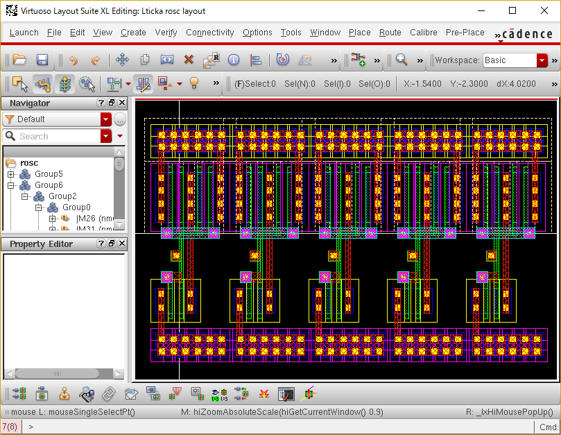
- Group the current-controlled inverter and generate 4 copies of it. Thus, you obtain the five current-controlled inverters. You can copy the layout by using the copy button on the toolbar or pressing c-key.
- Align the top or bottom of the current-controlled inverters by using the align button on the toolbar.

